Video Future AMD processors may function domain-specific accelerators – even some created by third events, in response to senior execs on the chip store.
Talking with AMD CTO Mark Papermaster in a video launched Wednesday, senior vp Sam Naffziger careworn the significance of chiplet standardization. You possibly can watch all 25 minutes under.
“Area-specific accelerators, that is one of the simplest ways to have the perfect efficiency per watt per greenback. So it’s completely important to progress. You possibly can’t afford to do a particular product for every one in every of these domains, so what we are able to do is have a chiplet ecosystem – a library basically,” Naffziger defined.
He was referring to Common Chiplet Interconnect Categorical (UCIe) – an open commonplace for chiplet communications that, since its creation in early 2022, has gained vast help from key trade gamers together with AMD, Arm, Intel, and Nvidia, and plenty of different smaller names too.
AMD has been on the forefront of chiplet architectures for the reason that launch of its first-gen Ryzen and Epyc processors in 2017. Since then, the Home of Zen’s chiplet library has advanced to incorporate a number of compute, I/O, and graphics dies, which it combines and packages in its client and datacenter processors.
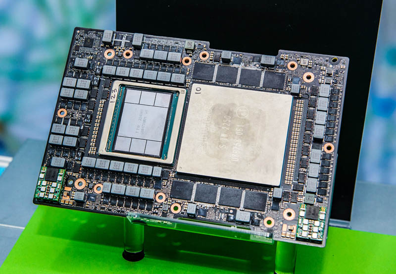
An instance of this method might be present in AMD’s Intuition MI300A APUs, launched in December 2023 and packing 13 particular person chiplets – 4 I/O dies, six GPU dies, and three CPU dies – together with eight stacks of HBM3 reminiscence.
Naffziger urged that sooner or later, requirements like UCIe may see chiplets constructed by third events make their method into AMD packages. He talked about silicon photonic interconnects – a tech which will ease bandwidth bottlenecks – as having potential to convey third-party chiplets into AMD merchandise.
Naffziger argued that and not using a low-power die-to-die interconnect, the expertise is not viable.
“You bolt optical on since you need huge bandwidth. So, you want low-energy per bit for that to make sense and in-package chiplets are the best way to get the bottom vitality interfaces,” he defined, including that he thinks that the transfer to co-packaged optics is “coming.”
To this finish, a number of silicon photonics startups are already pushing merchandise that just do that. For instance, Ayar Labs has developed a UCIe-compatible photonics chiplet that was built-in right into a prototype graph-analytics accelerator constructed by Intel final yr.
Whether or not third-party chiplets – photonics or in any other case – make their method into AMD merchandise stays to be seen. As we have beforehand reported, standardization is only one of many challenges that must be overcome to permit heterogeneous multi-die chips. We have requested AMD for extra info on its chiplet technique, and can let you already know if we hear something again.
AMD has made its chiplets obtainable to rival chipmakers earlier than. Intel’s Kaby Lake-G elements, launched in 2017, featured Chipzilla’s Eighth-gen cores together with AMD’s RX Vega GPU. The half just lately resurfaced in a NAS board from Topton. ®